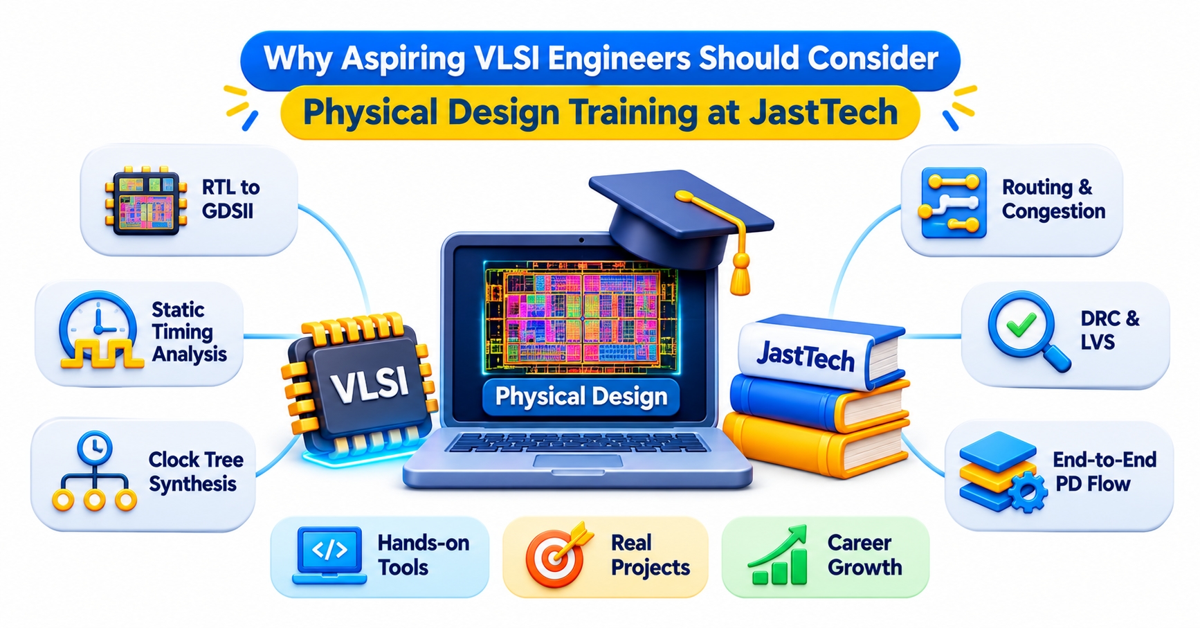
A chip can pass every functional simulation and still be unusable because one wire is too long, one clock edge arrives late, or one region of metal is packed too tightly. None of that shows up at the RTL stage. It surfaces in physical design, which is why physical design training deserves a serious look from anyone planning a VLSI career.
Many freshers hear that VLSI is hard to break into, but few are told which part of the flow to start with. The answer is less obvious than it sounds.
From RTL to GDSII: What Physical Design Really Involves
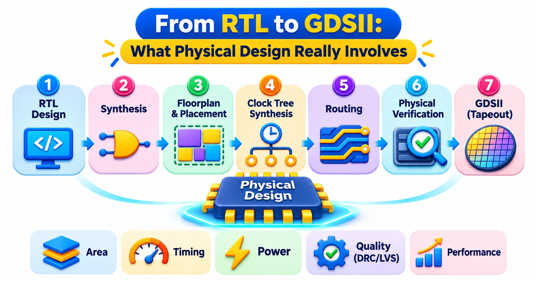
Physical design is the stage where a chip’s logical description becomes a physical layout that a foundry can manufacture. The logical description is called a netlist. It is simply a list of gates and the connections between them. It says nothing about where each gate sits on silicon or how the wires run between them.
That gap is what physical design fills. The work moves through a sequence of stages, and each one depends on the one before it:
Floorplanning decides the chip’s outline, where large blocks such as memories sit, and where the pins go.
Power planning builds the grid of power and ground lines that feeds every cell.
Placement puts millions of standard cells into legal positions while keeping connected cells close together.
Clock tree synthesis distributes the clock signal so every flip-flop sees it at nearly the same time.
Routing draws the actual metal wires between cells across multiple layers.
Signoff checks confirm the design meets timing, power, and manufacturing rules before it is released as a GDSII file.
The same netlist can turn into very different chips depending on these decisions. One implementation may run faster but draw more power. Another may be smaller but impossible to route cleanly. Physical design is the discipline of balancing those trade-offs, usually under tight schedules.
The work happens inside tools from the major EDA vendors, such as Synopsys (IC Compiler II and Fusion Compiler), Cadence (Innovus), and Siemens EDA. Engineers at semiconductor product companies, design service firms, and IP houses use them daily. The tools are powerful, but they are not magic. They follow constraints and settings that an engineer must understand, and that understanding is what separates someone who can run a flow from someone who can fix one when it breaks.
This is also why physical design is a good lens on VLSI as a whole. To do it well, you have to understand digital logic, timing, power, and manufacturing constraints at the same time. Few other roles pull so many threads together.
Why Physical Design Training Makes Sense for Aspiring VLSI Engineers
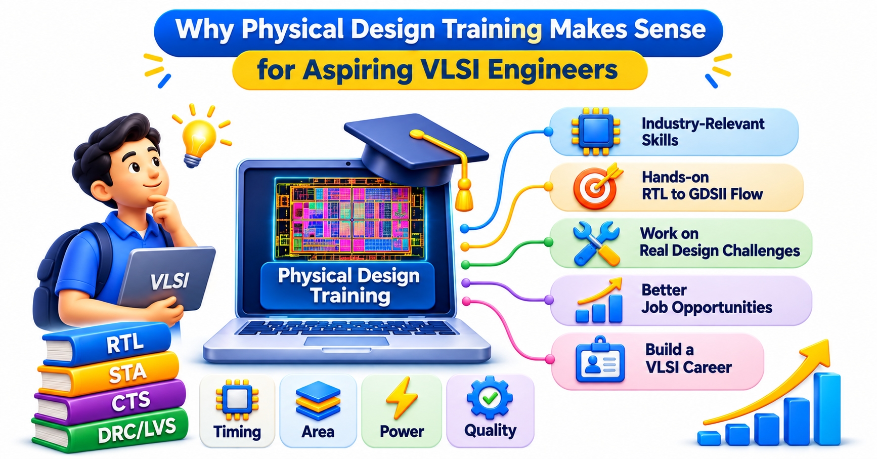
VLSI work splits broadly into front-end and back-end. Front-end roles, such as RTL design and verification, deal with what a chip does. Back-end roles, including physical design, static timing analysis, and physical verification, deal with how that logic becomes real silicon. Design for testability and analog layout sit alongside both.
Physical design is a sensible entry point for several reasons. Every digital chip, whatever its application, has to be implemented physically, so the skill is not tied to one product trend. Electronics and electrical graduates usually already have the fundamentals, such as CMOS basics and digital design, that the work builds on. And the knowledge compounds. Someone who understands placement, clock trees, and timing closure can move toward STA, physical verification, power analysis, or CAD automation without starting over.
There is also a practical problem with learning this on your own. The industry-grade tools are licensed software, and most students never get to touch them in college. Reading about congestion is very different from seeing a congestion map light up red in a real run and working out why. Hands-on exposure is the part that is hardest to replicate from textbooks and videos, and it is the strongest argument for structured training.
A word of honesty belongs here. Training does not guarantee a job. Hiring depends on your fundamentals, how well you explain your project work, and the openings available at the time. What a good program can do is shorten the distance between knowing the theory and being comfortable discussing real flows in an interview.
It can also help you decide early whether the work suits you. Physical design rewards patience. A single run can take hours, a small constraint change can ripple through the whole design, and the debugging is detective work. Some people find that frustrating. Others find it the most satisfying part of engineering. Finding out which camp you belong to during training is far cheaper than finding out on your first job.
The Skills a Good Physical Design Course Should Actually Build
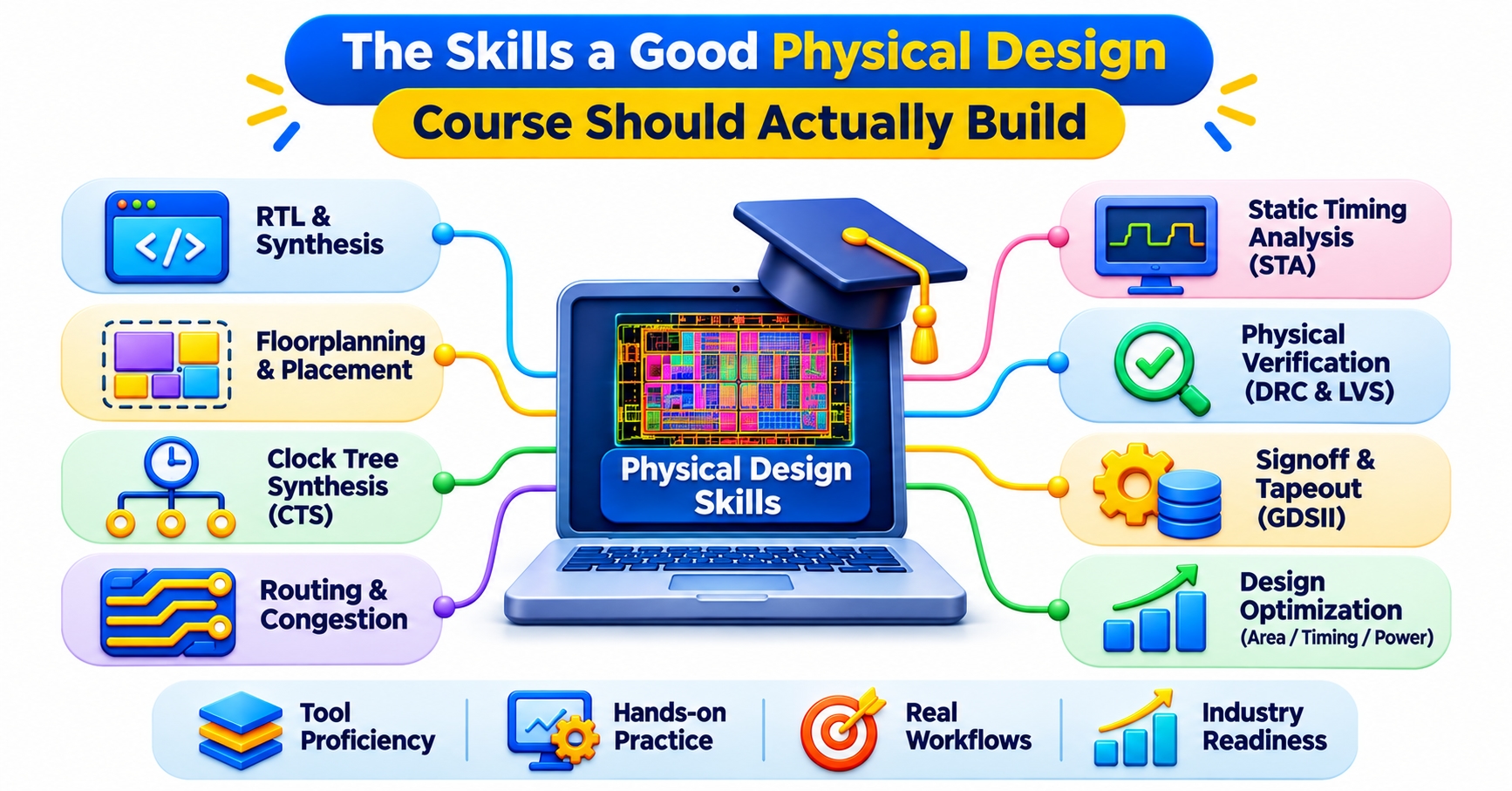
Learning the stage names is the easy part. What makes a candidate useful is a set of underlying skills, and these are worth checking for in any course you consider.
Static timing analysis. STA is effectively the language of physical design. Setup and hold checks, slack, clock uncertainty, and path groups come up in almost every discussion about whether a design is “closing.” If a course treats timing as an afterthought, that is a warning sign.
Digital and CMOS fundamentals. Why does a hold violation appear after clock tree synthesis? Why does a long wire slow a signal? These answers come from basic circuit behavior, and interviewers test them often.
Linux and scripting. Tools are driven through command lines and scripts. Comfort with Linux, TCL, and some Python lets you automate repetitive runs and read large reports without getting lost.
Constraint handling. Design constraints, usually written in SDC files, tell the tools what the chip is supposed to achieve. A wrong clock definition can send you chasing violations that do not exist.
Power integrity. IR drop and electromigration are about whether the power grid can really deliver current under load. Beginners often skip this until it bites them.
Physical verification. DRC checks manufacturing rules, LVS checks that the layout matches the schematic, and antenna checks catch charge-related issues during fabrication. Understanding them closes the loop between layout and fabrication.
Report reading. This is the most underrated skill. A timing report is a story about a path. Learning to read where the delay accumulates, and why, is what makes debugging faster.
Notice that none of these skills is about memorizing menus. Tool interfaces change between versions, and flows differ between companies. The reasoning behind a fix stays useful. A course that spends most of its time teaching which button to press will leave you stranded the first time you meet a different tool or a different problem.
When you evaluate a syllabus, look for a balance. Theory without tool practice leaves you unable to work, and tool practice without theory leaves you unable to explain what you did.
What a Real Physical Design Project Feels Like
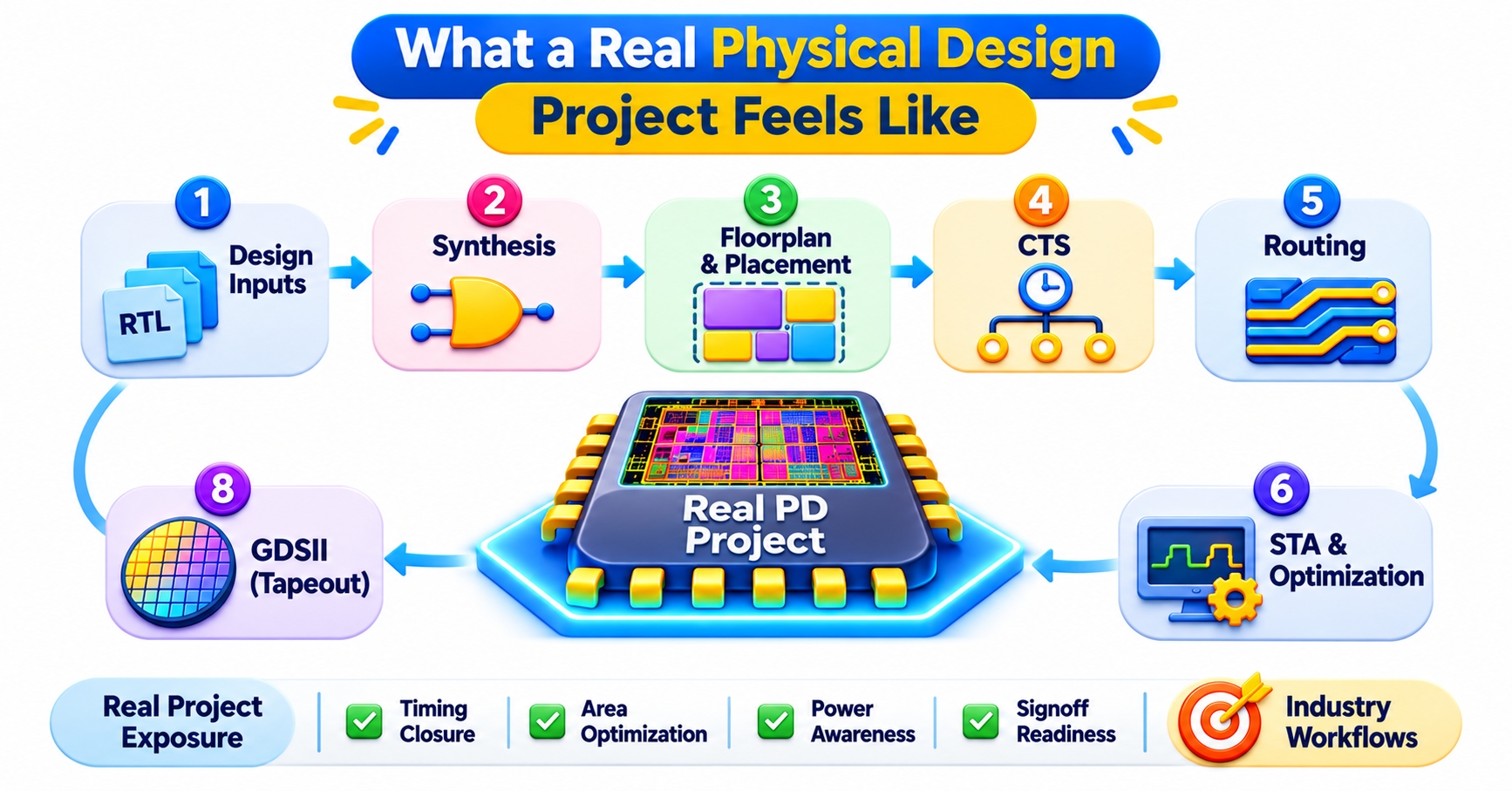
To see why the skills above matter, picture a hypothetical block: a mid-sized signal-processing module with a few memory macros and a clock that must run at a demanding frequency. This is an illustration, not a case study, but the pattern is typical of what learners meet in project work.
The first run through placement shows heavy congestion near the memories. The cause is not a mystery once you look at the floorplan. The macros were placed too close together, leaving narrow channels where too many wires need to pass. The fix is to move the macros, add blockages around them, and rerun. Notice that the problem was created at floorplanning but only became visible several stages later.
After clock tree synthesis, the setup picture looks acceptable, but hold violations appear on short paths. Those paths were fine before because the clock was treated as ideal. Now real clock skew exposes them. The engineer inserts delay cells or buffers on the affected paths, which solves hold but may eat into setup slack elsewhere.
Then routing begins, and a batch of DRC violations appears around dense areas. Some can be cleared by rerouting. Others need small changes to cell spacing. After each fix, the timing is checked again, because a rerouted wire has a new length and a new delay.
Eventually the design closes, and then a late change arrives. A designer modifies one small piece of logic. Instead of restarting, the physical design engineer makes an engineering change order, or ECO, touching only the affected cells and wires, and re-verifies the result.
Here is what this story teaches. Every fix has a side effect. Problems appear far from where they started. And the job is less about running a flow once than about iterating intelligently. A learner who has walked through even one such cycle, with an experienced person explaining each decision, will answer interview questions about congestion, skew, or ECOs far more convincingly than someone who has only read definitions.
That is why project work is the core of any good program, not a decorative extra. Ask what the project design looks like, how many stages you will carry through yourself, and whether you will see failures, not just clean runs.
Mistakes Beginners Make When Learning Physical Design
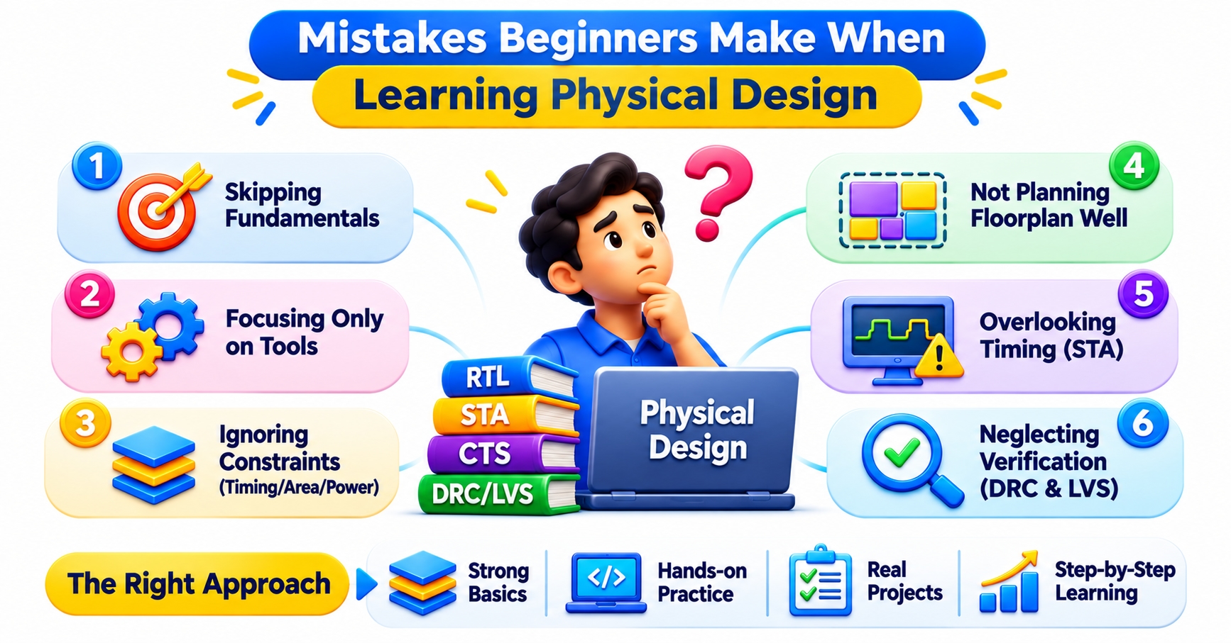
Most of the common errors come from treating the subject as a procedure instead of a problem-solving craft.
Memorizing commands without understanding intent. A learner can recite the tool commands for placement and still be unable to explain why a placement is poor. When asked “what would you change if utilization is too high?”, the memorized sequence does not help.
Skipping timing fundamentals. Some candidates rush into the tool flow before they are comfortable with setup and hold. Everything later becomes confusing because slack numbers carry no meaning for them.
Learning stages in isolation. Floorplanning, placement, and routing are connected. Treating them as separate topics hides the cause-and-effect chain described earlier, where an early decision creates a late problem.
Ignoring physical verification and power. Because timing gets most of the attention, DRC, LVS, and IR drop are often left to the end. Employers expect at least working familiarity with all of them.
Avoiding scripting. Engineers who cannot write a small TCL script to extract numbers from reports end up doing manual work that others automate. Basic scripting is a quiet but real advantage.
Reading results without questioning them. A tool saying “zero violations” is not the end. Was the constraint file correct? Were all corners and modes analyzed? Good engineers distrust a clean result until they know what it covered.
Expecting mastery from a short course. Physical design takes practice. A solid course gives you the foundation and a project to talk about. Competence grows through repeated runs on different designs, over months, not weeks.
There is also a mistake that has nothing to do with technique: choosing a program based on promises. If a course advertises guaranteed placement or promises job-readiness in an unrealistically short time, ask hard questions. A reliable program talks about what you will learn and practice, not what you will be handed.
The encouraging part is that all of these mistakes are avoidable. They mostly come from missing guidance, not missing talent, and guidance is exactly what structured training with experienced mentors is meant to provide.
How to Judge a VLSI Training Institute, and Where JastTech Fits

Choosing where to train matters nearly as much as deciding to train. Plenty of institutes teach VLSI, and the differences show up in details. When comparing any VLSI training institute in India, these questions are worth asking:
Does the curriculum cover the full flow, from floorplanning to signoff, or only a few stages?
Will you work on industry-standard EDA tools, and for how many hours?
Is there a project on a realistic block, and will you run it end to end?
Do the trainers have actual industry experience in physical design?
Is STA taught in depth, not as a single lecture?
Is there interview preparation based on the questions that physical design roles actually ask?
Is the institute honest about what training can and cannot promise?
You can usually learn a lot by asking for a sample session, a syllabus breakdown, or a conversation with a trainer. A program that is confident in its teaching will not mind the scrutiny.
JastTech runs a dedicated physical design program alongside other VLSI and technology courses, which means a learner can study the subject in a setting built around it and not treat it as one chapter of a broad VLSI overview. The sensible approach is the same one you would use for any institute: read the module list, compare it with the checklist above, and ask direct questions about tools, project scope, and trainer background before enrolling. If the answers match what you need, it is a reasonable place to build your foundation.
Location and format matter too. Some learners need classroom access and some prefer online flexibility, and batch size affects how much individual attention you will get when a run fails at midnight and you need to know why.
Finally, think about what you plan to do after the course. Training works best when it is followed by practice: rerunning projects with different constraints, reading timing reports from other designs, and preparing to explain every decision you made. The institute gives you the base. The habit of curiosity afterward is yours to build.
Conclusion
Physical design is where a chip stops being an idea and becomes something a foundry can build, which makes physical design training a sensible starting point for engineers who want hands-on work close to silicon. The right program teaches the full flow, the reasoning behind every fix, and the discipline of reading reports carefully. Pick one that does, and the tools become learnable. What remains is practice, patience, and a few thousand timing paths.